|
|
| (같은 사용자의 중간 판 3개는 보이지 않습니다) |
| 1번째 줄: |
1번째 줄: |
| − | SAW-핸드폰DPX | + | SAW 듀플렉서 |
| | <ol> | | <ol> |
| | <li> [[전자부품]] | | <li> [[전자부품]] |
| | <ol> | | <ol> |
| | <li> [[SAW대문]] | | <li> [[SAW대문]] |
| | + | <li> [[듀플렉서]] |
| | <ol> | | <ol> |
| − | <li> [[SAW-핸드폰DPX]] - 이 페이지 | + | <li> [[SAW 듀플렉서]] - 이 페이지 |
| | + | <ol> |
| | + | <li> [[9.5x7.5 SAW 듀플렉서]] |
| | + | <li> [[5.0x5.0 SAW 듀플렉서]] |
| | + | <li> [[3.8x3.8 SAW 듀플렉서]] |
| | + | <li> [[3.2x2.5 SAW 듀플렉서]] |
| | + | <li> [[3.0x2.5 SAW 듀플렉서]] |
| | + | <li> [[2.5x2.0 SAW 듀플렉서]] |
| | + | <li> [[2.0x1.6 SAW 듀플렉서]] |
| | + | <li> [[1.8x1.4 SAW 듀플렉서]] |
| | + | <li> [[1.55x1.15 SAW 듀플렉서]] |
| | + | <li> [[1.4x1.1 SAW 듀플렉서]] |
| | + | </ol> |
| | <li>참고 | | <li>참고 |
| | <ol> | | <ol> |
| 12번째 줄: |
25번째 줄: |
| | <li> [[PAMiD]] | | <li> [[PAMiD]] |
| | </ol> | | </ol> |
| | + | </ol> |
| | + | <li>참고 |
| | + | <ol> |
| | + | <li> [[필터 정격전력]] 내전력, 허용전력 |
| | </ol> | | </ol> |
| | </ol> | | </ol> |
| 25번째 줄: |
42번째 줄: |
| | image:u_100_016.jpg | | image:u_100_016.jpg |
| | image:u_100_017.jpg | Tx, Rx필터로 duplexer 만드는 법 | | image:u_100_017.jpg | Tx, Rx필터로 duplexer 만드는 법 |
| − | </gallery>
| |
| − | </ol>
| |
| − | </ol>
| |
| − | <li>9.5x7.5mm
| |
| − | <ol>
| |
| − | <li>3.0x3.0mm 필터를 사용함.
| |
| − | <ol>
| |
| − | <li>삼성전기, 개발품(?) 모델명 모름
| |
| − | <ol>
| |
| − | <li>이 상태로 있길래
| |
| − | <gallery>
| |
| − | image:saw_dpx9575_02_001.jpg
| |
| − | image:saw_dpx9575_02_002.png
| |
| − | image:saw_dpx9575_02_003.jpg
| |
| − | </gallery>
| |
| − | <li>깡통을 벗기니
| |
| − | <gallery>
| |
| − | image:saw_dpx9575_02_004.jpg
| |
| − | </gallery>
| |
| − | <li>3.0x3.0mm 쏘필터를 다시 납땜해서
| |
| − | <gallery>
| |
| − | image:saw_dpx9575_02_005.jpg | 왼쪽 881, 오른쪽 836
| |
| − | image:saw_dpx9575_02_006.png
| |
| − | </gallery>
| |
| − | <li>쏘필터 뚜껑을 벗기니
| |
| − | <gallery>
| |
| − | image:saw_dpx9575_02_007.jpg
| |
| − | image:saw_dpx9575_02_008.jpg | 왼쪽 881, 오른쪽 836
| |
| − | image:saw_dpx9575_02_009.jpg | X881 50
| |
| − | image:saw_dpx9575_02_010.jpg | X836 50
| |
| − | image:saw_dpx9575_02_011.jpg
| |
| − | </gallery>
| |
| − | </ol>
| |
| − | <li>삼성전기, 개발품(?)
| |
| − | <ol>
| |
| − | <li>이 상태로 발견. X881XH, X836XH로 추정. 2000년 172로트
| |
| − | <gallery>
| |
| − | image:saw_dpx9575_03_001.jpg
| |
| − | image:saw_dpx9575_03_002.png
| |
| − | </gallery>
| |
| − | </ol>
| |
| − | </ol>
| |
| − | <li>후지쯔(Fujitsu Media Devices Limited), FAR-D5CC-881M50-D1A4
| |
| − | <ol>
| |
| − | <li>제품규격서
| |
| − | <ol>
| |
| − | <li> - 12p
| |
| − | <li> - 15p
| |
| − | </ol>
| |
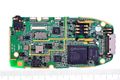
| − | <li> [[StarTAC]] 휴대폰에서
| |
| − | <gallery>
| |
| − | image:startac01_002.jpg | B면
| |
| − | image:startac01_006.jpg | [[PAM]] [[커플러]]
| |
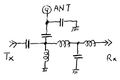
| − | image:startac01_005.jpg | 아래:ANT, 왼쪽:Tx, 오른쪽:Rx
| |
| − | image:startac01_007.jpg
| |
| − | </gallery>
| |
| − | </ol>
| |
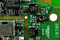
| − | <li>삼성전기 X836KP - 2001년 제품
| |
| − | <ol>
| |
| − | <li>어떤 측정치구
| |
| − | <gallery>
| |
| − | image:saw_dpx9575_00_001.jpg
| |
| − | </gallery>
| |
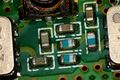
| − | <li>자재 및 공정
| |
| − | <ol>
| |
| − | <li>사용 패키지와 리드(8.0x6.0mm) 비교
| |
| − | <gallery>
| |
| − | image:lid_ausn10_005.jpg
| |
| − | image:lid_ausn10_006.jpg
| |
| − | image:lid_ausn10_007.jpg
| |
| − | </gallery>
| |
| − | <li>융착 결과 - AuSn 두께가 30um으로 두꺼워야 하는 이유. 패키지가 크면 warpage가 커, 빈공간을 메워야 하므로
| |
| − | <gallery>
| |
| − | image:lid_ausn10_008.jpg
| |
| − | image:lid_ausn10_009.jpg
| |
| − | </gallery>
| |
| − | </ol>
| |
| − | <li>
| |
| − | <li>2017.02 출시 샤오미 [[Redmi Note 4X]] 스마트폰에서 나온 1.8x1.4mm 및 1.55x1.15mm 크기와 비교
| |
| − | <gallery>
| |
| − | image:saw_dpx9575_02_012.jpg | 9.5x7.5mm vs 1.8x1.4mm
| |
| − | image:saw_dpx9575_02_013.jpg | 9.5x7.5mm vs 1.55x1.15mm
| |
| − | </gallery>
| |
| − | <li>[[포켓WiFi]]에서 사용된 2.0x1.6mm 제품과 비교하기 위해 분해
| |
| − | <ol>
| |
| − | <li>비교 사진
| |
| − | <gallery>
| |
| − | image:saw_dpx9575_01_001.jpg
| |
| − | image:saw_dpx9575_01_002.jpg
| |
| − | image:saw_dpx9575_01_003.jpg
| |
| − | image:saw_dpx9575_01_004.jpg
| |
| − | image:saw_dpx9575_01_005.jpg
| |
| − | </gallery>
| |
| − | <li>칩 전체
| |
| − | <gallery>
| |
| − | image:saw_dpx9575_01_006.jpg | Rx(881.5MHz)
| |
| − | image:saw_dpx9575_01_007.jpg | Tx(836.5MHz)
| |
| − | </gallery>
| |
| − | <li>확대
| |
| − | <gallery>
| |
| − | image:saw_dpx9575_01_008.jpg
| |
| − | image:saw_dpx9575_01_009.jpg
| |
| − | </gallery>
| |
| − | <li>더 확대
| |
| − | <gallery>
| |
| − | image:saw_dpx9575_01_010.jpg | 주기: 4.27um - Rx(881.5MHz)
| |
| − | image:saw_dpx9575_01_011.jpg | 위쪽 주기: 4.56um - Tx(836.5MHz)
| |
| − | </gallery>
| |
| − | <li>무라타 2016과 비교
| |
| − | <gallery>
| |
| − | image:saw_dpx9575_01_012.jpg
| |
| − | image:saw_dpx9575_01_013.jpg
| |
| − | </gallery>
| |
| − | <li>Rx 칩에서, HWP 폰트(유니코드 문자코드 263B, Black Smiling Face)로 만든 패턴인듯.
| |
| − | <gallery>
| |
| − | image:saw_dpx9575_01_014.jpg
| |
| − | </gallery>
| |
| − | </ol>
| |
| − | </ol>
| |
| − | </ol>
| |
| − | <li>5.0x5.0mm
| |
| − | <ol>
| |
| − | <li>Fujitsu
| |
| − | <ol>
| |
| − | <li>제품규격서
| |
| − | <ol>
| |
| − | <li> - 9p
| |
| − | </ol>
| |
| − | <li>2005.05 제조 [[싸이버뱅크 CP-X310]] PDA폰
| |
| − | <gallery>
| |
| − | image:cp_x310_028_001.jpg
| |
| − | image:cp_x310_029.jpg | M5 마킹
| |
| − | </gallery>
| |
| − | <li> [[LG-SD1250]] 2003년 3월 제조된 [[핸드폰]]에서
| |
| − | <ol>
| |
| − | <li>외관
| |
| − | <gallery>
| |
| − | image:lg_sd1250_006.jpg
| |
| − | image:lg_sd1250_007.jpg | RF단
| |
| − | image:lg_sd1250_008.jpg | Fujitsu, 836.5/881.5MHz Duplexer, 5.0x5.0mm
| |
| − | </gallery>
| |
| − | <li>내부
| |
| − | <gallery>
| |
| − | image:lg_sd1250_008_001.jpg | 알루미늄 웨지 [[와이어본딩]]
| |
| − | image:lg_sd1250_008_002.jpg | 실버에폭시 다이본딩
| |
| − | image:lg_sd1250_008_003.jpg | MHA622-03, 다이 크기 2.37x1.96mm
| |
| − | </gallery>
| |
| − | <li>불에 달궈 다이를 뜯음
| |
| − | <gallery>
| |
| − | image:lg_sd1250_008_004.jpg | 다이를 뜯어내기 위해 빨갛게 달군 후(검정 물질은 땜납 Sn이 산화되면 이렇게 부피가 커지는 듯)
| |
| − | image:lg_sd1250_008_005.jpg | 측면 다이싱
| |
| − | </gallery>
| |
| − | </ol>
| |
| − | </ol>
| |
| − | </ol>
| |
| − | <li>3.8x3.8mm
| |
| − | <ol>
| |
| − | <li>삼성전기
| |
| − | <ol>
| |
| − | <li>LTCC, 캐비티 패키지, KYH
| |
| − | <gallery>
| |
| − | image:saw_dpx3838_01_001.jpg | 이 상태로 존재함
| |
| − | image:saw_dpx3838_01_002.jpg
| |
| − | </gallery>
| |
| − | <li>팬택 & 큐리텔 [[PT-L2200]] 피처폰에서
| |
| − | <ol>
| |
| − | <li>SFXG65KC401, Korea PCS(Tx 1765MHz Rx 1855MHz), China 2006 190lot
| |
| − | <gallery>
| |
| − | image:pt_l2200_013.jpg | FCI 7214 [[PAM]] -> 무라타 [[아이솔레이터]] -> DPX
| |
| − | image:pt_l2200_014.jpg
| |
| − | image:pt_l2200_015.jpg | LTCC 6층 적층
| |
| − | </gallery>
| |
| − | <li>뚜껑을 벗기고
| |
| − | <gallery>
| |
| − | image:pt_l2200_016.jpg
| |
| − | image:pt_l2200_017.jpg | 빨강화살표 전극 - 괜히 넣었다. isolation 특성을 저해한다. 파랑화살표 본딩 - Rx와 Tx를 연결하는 와이어를 공통으로 찍었기 때문에 isolation 특성을 저해한다.
| |
| − | image:pt_l2200_018.jpg | XG65KC4, KYH 씨 설계로 추정
| |
| − | </gallery>
| |
| − | <li>불에 태우면
| |
| − | <gallery>
| |
| − | image:pt_l2200_018_001.jpg
| |
| − | image:pt_l2200_018_002.jpg
| |
| − | image:pt_l2200_018_003.jpg
| |
| − | </gallery>
| |
| − | </ol>
| |
| − | <li>K-PCS 내전력, 50도씨에서 1W 5만시간 이상
| |
| − | </ol>
| |
| − | <li>Fujitsu
| |
| − | <ol>
| |
| − | <li>FAR-D5CF-881M50-D1F1
| |
| − | <ol>
| |
| − | <li>2006.02 출시, 팬택, SKY 주크박스 [[IM-U110]] 피처폰
| |
| − | <ol>
| |
| − | <li>외관, F1 마킹은 FAR-D5CF-881M50-D1F1 이다.
| |
| − | <gallery>
| |
| − | image:im_u110_018.jpg
| |
| − | image:im_u110_018_001.jpg | [[LTCC 제품]] 패키지 위에 가장자리에만 AuSn[[솔더]]가 발라진 평탄한 뚜껑(lid)를 눌러서 납땜하였다.
| |
| − | </gallery>
| |
| − | <li>뚜껑(lid)을 벗기면
| |
| − | <gallery>
| |
| − | image:im_u110_018_002.jpg | [[Al 웨지 와이어본딩]]
| |
| − | image:im_u110_018_003.jpg | 패키지 4코너에 접지용 비아가 있다.
| |
| − | </gallery>
| |
| − | <li>다이 관찰
| |
| − | <gallery>
| |
| − | image:im_u110_018_004.jpg | Tx 다이에는 5개 본딩, Rx 다이는 10개 본딩
| |
| − | image:im_u110_018_005.jpg | 유기물 오염
| |
| − | </gallery>
| |
| − | <li> [[EMI]] 차폐를 강화시킨 밑면 [[접지]] 패턴
| |
| − | <gallery>
| |
| − | image:im_u110_018_006.jpg | ANT Tx Rx 단자 위치. 패키지 밑면 T자 접지에 납땜하지 않았다.
| |
| − | image:im_u110_018_007.jpg | 갈아낸 후 전극 모양
| |
| − | </gallery>
| |
| − | <li>패키지를 가열한 후. 와이어가 연결된 전극은 [[SAW필터에서 초전성]] 때문에 쉽게 녹는다.
| |
| − | <gallery>
| |
| − | image:im_u110_018_008.jpg
| |
| − | image:im_u110_018_009.jpg
| |
| − | </gallery>
| |
| − | </ol>
| |
| − | </ol>
| |
| − | </ol>
| |
| − | <li>Matsushita Electronic Components Co. (Panasonic)
| |
| − | <ol>
| |
| − | <li>데이타시트
| |
| − | <li>2006.10 출시 삼성 월드로밍 [[SCH-V920]] 슬라이드 피처폰
| |
| − | <ol>
| |
| − | <li>기술정보
| |
| − | <ol>
| |
| − | <li>내부 패턴을 보면 Epcos 설계와 매우 유사
| |
| − | </ol>
| |
| − | <li>CDMA, Fc=836.5/881.5MHz, 모델명 EFSD836Mxx
| |
| − | <gallery>
| |
| − | image:sch_v920_025.jpg
| |
| − | image:sch_v920_025_001.jpg
| |
| − | image:sch_v920_025_002.jpg
| |
| − | image:sch_v920_025_003.jpg | D83FL 88 HR
| |
| − | image:sch_v920_025_004.jpg
| |
| − | image:sch_v920_025_005.jpg
| |
| − | </gallery>
| |
| − | <li>J-CDMA, fc=856.5/911.5MHz, 모델명 EFSD911MD1 또는 EFSD911MD2
| |
| − | <gallery>
| |
| − | image:sch_v920_026.jpg
| |
| − | image:sch_v920_026_001.jpg
| |
| − | image:sch_v920_026_002.jpg
| |
| − | image:sch_v920_026_003.jpg | A8590G12P
| |
| − | </gallery>
| |
| − | </ol>
| |
| − | <li>2007년 팬택&큐리텔 스위블 피처폰 [[canU701D]]에서
| |
| − | <ol>
| |
| − | <li>외관
| |
| − | <gallery>
| |
| − | image:canu701d_011.jpg | Qualcomm RFT6100 Tx IC, FCI 7214 PAM, Matsushita EFSD1765D2S3 SAW DPX, FCI 7510 LNA, Qualcomm RFR6000 Rx IC
| |
| − | image:canu701d_012.jpg
| |
| − | image:canu701d_013.jpg | EFSD1765D2S3, Matsushita Electronic Components Co., Ltd.(Osaka) LCR Device Company, Ceramic Business Unit, 2003년 규격서에서
| |
| − | </gallery>
| |
| − | <li>측정
| |
| − | <gallery>
| |
| − | image:canu701d_024.jpg
| |
| − | image:canu701d_025.png
| |
| − | </gallery>
| |
| − | <li>기밀성 테스트(문제 없다.) 및 온도 특성
| |
| − | <gallery>
| |
| − | image:canu701d_026.jpg
| |
| − | image:canu701d_027.jpg
| |
| − | image:canu701d_028.png | 약 130도씨
| |
| − | </gallery>
| |
| − | <li>납땜 단자 고착 강도
| |
| − | <gallery>
| |
| − | image:canu701d_029.jpg | 땜납이 떨어진다. LTCC 전극 고착강도가 무척 높다.
| |
| − | </gallery>
| |
| − | <li>다이
| |
| − | <gallery>
| |
| − | image:canu701d_030.jpg | AuSn 리드를 칼로 뜯어낸 후
| |
| − | image:canu701d_031.jpg | 리버스(칩을 2nd 본딩), 알루미늄 웨지 와이어본딩
| |
| − | image:canu701d_032.jpg | 모든 IDT가 C 직렬연결
| |
| − | </gallery>
| |
| − | <li>현미경 촬영 거리를 줄이기 위해, 다이를 뜯어내기 위해, 빨갛게 달궈 Ag 에폭시 접착력을 떨어뜨려 다이를 뜯어냄
| |
| − | <gallery>
| |
| − | image:canu701d_033.jpg | 우물 자국은 이물질이 폭발한 듯
| |
| − | image:canu701d_034.jpg | 단단한 전극인듯, 산화물 보호막이 있는 듯
| |
| − | </gallery>
| |
| − | </ol>
| |
| − | </ol>
| |
| − | <li>SAWTEK 856331, CDMA용 850MHz
| |
| − | <ol>
| |
| − | <li>규격서 - 6p
| |
| − | <li> [[SAW-핸드폰DPX]]
| |
| − | <ol>
| |
| − | <li>SAWTEK 856331, W마크가 이 기종이다. 1997년 141일차, 생산지C
| |
| − | <gallery>
| |
| − | image:ms500_01_026.jpg | [[안테나]]와 DPX와의 경로 중간에 [[안테나 커넥터 스위치]]가 있다.
| |
| − | </gallery>
| |
| − | <li>주파수 특성
| |
| − | <gallery>
| |
| − | image:ms500_01_027.jpg
| |
| − | image:ms500_01_027_001.png | 광대역 특성
| |
| − | image:ms500_01_027_002.png | 통과대역 특성
| |
| − | image:ms500_01_027_003.png | 3포트 반사 특성
| |
| − | image:ms500_01_027_004.png | 3포트 매칭
| |
| − | image:ms500_01_027_005.png | Tx/Rx ladder 필터의 지연시간 약 20nsec
| |
| − | </gallery>
| |
| − | <li>뚜껑 열기(delidding)
| |
| − | <gallery>
| |
| − | image:ms500_01_028.jpg | [[Au 볼 와이어본딩]]에서 와이어가 [[직선 도선 인덕터]]로 동작한다.
| |
| − | image:ms500_01_029.jpg | 왼쪽과 오른쪽 두 패턴 사이를 [[차폐]]하기 위한 Y자 접지 패턴이 이채롭다.
| |
| − | </gallery>
| |
| − | <li>패턴
| |
| − | <gallery>
| |
| − | image:ms500_01_030.jpg | 위쪽이 Tx 패턴일 듯
| |
| − | image:ms500_01_031.jpg | [[정전기]] 파괴
| |
| − | image:ms500_01_032.jpg | 정전기 파괴
| |
| − | image:ms500_01_033.jpg | 글꼴 설계, M자는 [[Copyright]]
| |
| − | </gallery>
| |
| − | </ol>
| |
| − | </ol>
| |
| − | </ol>
| |
| − | <li>3.2x2.5mm
| |
| − | <ol>
| |
| − | <li>무라타 SAW UMTS 2100(Tx 1920-1980, Rx 2110-2170) DPX, 3.2x2.5mm [[LTCC 기판]] 캐비티 구리전극, 2칩, 플립본딩, AuSn 실링
| |
| − | <ol>
| |
| − | <li>2008년 1월 제조된 [[LG-SH170]] 슬라이드 피처폰
| |
| − | <ol>
| |
| − | <li>리드 실링이 틀어져 있다. (힘들게 하나씩 리드를 누르면서 실링했다는 뜻)
| |
| − | <gallery>
| |
| − | image:sh170_052.jpg
| |
| − | image:sh170_053.jpg
| |
| − | image:sh170_054.jpg
| |
| − | </gallery>
| |
| − | <li>AuSn 실링
| |
| − | <gallery>
| |
| − | image:sh170_055.jpg
| |
| − | image:sh170_056.jpg | 검정색 칩, 이젝트핀 자국
| |
| − | image:sh170_057.jpg
| |
| − | image:sh170_058.jpg | 기판 구리전극이 뜯어졌다. 칩에서 보호막 두께가 달라 색상이 달리 보인다.
| |
| − | </gallery>
| |
| − | <li>다이 패턴
| |
| − | <gallery>
| |
| − | image:sh170_059.jpg | W734-A1
| |
| − | image:sh170_060.jpg
| |
| − | image:sh170_061.jpg
| |
| − | image:sh170_062.jpg | 융착온도 때문에 금속 확산
| |
| − | </gallery>
| |
| − | <li>어떤 칩 [[다이싱]] 단면
| |
| − | <gallery>
| |
| − | image:sh170_063.jpg | 한쪽면
| |
| − | image:sh170_064.jpg | 같은 칩에서 그 반대 한쪽면
| |
| − | image:sh170_065.jpg
| |
| − | </gallery>
| |
| − | </ol>
| |
| − | <li>2008.04 제조 삼성 [[SPH-W4700]] 슬라이드 피처폰
| |
| − | <ol>
| |
| − | <li>외관
| |
| − | <gallery>
| |
| − | image:w4700_020.jpg
| |
| − | image:w4700_021.jpg | Au-Sn [[솔더]]로 리드 실링
| |
| − | </gallery>
| |
| − | <li> [[플립본딩]]
| |
| − | <gallery>
| |
| − | image:w4700_022.jpg | 검정색 다이, 다이 중앙에 이젝트핀 자국
| |
| − | image:w4700_023.jpg
| |
| − | image:w4700_024.jpg | [[LTCC 기판]]은 구리전극에 캐비티 형태
| |
| − | </gallery>
| |
| − | <li>칩1, 유전체 보호막 때문에 웨이퍼 표면이 보라색으로 보임
| |
| − | <gallery>
| |
| − | image:w4700_025.jpg | W734-A1, 가중 weighting 전극
| |
| − | </gallery>
| |
| − | <li>칩2, 유전체 보호막 때문에 웨이퍼 표면이 보라색으로 보임
| |
| − | <gallery>
| |
| − | image:w4700_026.jpg | 가중 weighting 전극
| |
| − | </gallery>
| |
| − | </ol>
| |
| − | </ol>
| |
| − | </ol>
| |
| − | <li>3.0x2.5mm
| |
| − | <ol>
| |
| − | <li>엡코스
| |
| − | <ol>
| |
| − | <li>2009.06 출시 삼성 슬라이드위젯폰 [[SCH-B8850D]]
| |
| − | <ol>
| |
| − | <li>두 개 제품 외관
| |
| − | <gallery>
| |
| − | image:sch_b8850d_019.jpg
| |
| − | </gallery>
| |
| − | <li>위 사진에서 왼쪽에 있는 7662 마킹, 1765/1855MHz Korea PCS용
| |
| − | <gallery>
| |
| − | image:sch_b8850d_019_7662_001.jpg
| |
| − | image:sch_b8850d_019_7662_002.jpg | 주기 2.17um 1855MHz라면 4025m/sec
| |
| − | </gallery>
| |
| − | <li>오른쪽에 있는 A21 마킹, 836.5/881.5MHz용
| |
| − | <ol>
| |
| − | <li>다이 패턴
| |
| − | <gallery>
| |
| − | image:sch_b8850d_019_a21_001.jpg | 위치 1,2,3
| |
| − | image:sch_b8850d_019_a21_002.jpg | 위치 1 주기 4.38um 881MHz라면 3860m/sec
| |
| − | image:sch_b8850d_019_a21_003.jpg | 위치 2 주기 4.63um
| |
| − | image:sch_b8850d_019_a21_004.jpg | 위치 3 주기 4.825um 836MHz라면 4030m/sec
| |
| − | </gallery>
| |
| − | <li>다이 뒷면을 빨갛게 가열한 후
| |
| − | <gallery>
| |
| − | image:sch_b8850d_019_a21_005.jpg
| |
| − | image:sch_b8850d_019_a21_006.jpg
| |
| − | </gallery>
| |
| − | </ol>
| |
| − | </ol>
| |
| − | </ol>
| |
| − | <li>후지쯔
| |
| − | <ol>
| |
| − | <li>제품규격서
| |
| − | <ol>
| |
| − | <li> - 11p
| |
| − | </ol>
| |
| − | </ol>
| |
| − | <li>밸러스 Rx, SJB(송진백)
| |
| − | <gallery>
| |
| − | image:saw_dpx3025_01_001.jpg
| |
| − | </gallery>
| |
| − | </ol>
| |
| − | <li>2.5x2.0mm
| |
| − | <ol>
| |
| − | <li>와이솔
| |
| − | <ol>
| |
| − | <li>2010/10 삼성 [[GT-B6520]] 휴대폰에서
| |
| − | <ol>
| |
| − | <li>위치
| |
| − | <gallery>
| |
| − | image:gt_b6520_012.jpg | SAW 부품 1,2,3,4,5,6 위치
| |
| − | </gallery>
| |
| − | <li>2번 [[SAW-핸드폰DPX]] 2.5x2.0mm, 와이솔 제품
| |
| − | <gallery>
| |
| − | image:gt_b6520_016.jpg | 칩 두께가 서로 다르다.
| |
| − | image:gt_b6520_016_001.jpg | XG50PD5-MP6 Rx HJD
| |
| − | image:gt_b6520_016_002.jpg | XG50PD5-MP? Tx HJD
| |
| − | </gallery>
| |
| − | <li>3번 [[SAW-핸드폰DPX]] 2.5x2.0mm, 와이솔(?) 제품
| |
| − | <gallery>
| |
| − | image:gt_b6520_017.jpg | 칩 두께가 서로 다르다.
| |
| − | </gallery>
| |
| − | </ol>
| |
| − | </ol>
| |
| − | <li>Epcos
| |
| − | <ol>
| |
| − | <li>2011.02 출시 삼성 와이즈 [[SHW-A240S]] 폴더 피처폰
| |
| − | <ol>
| |
| − | <li>W-CDMA Band1(1950/2140MHz), Epcos 제조, 모델명 B7696(B39212B7696M810)
| |
| − | <ol>
| |
| − | <li>외관
| |
| − | <gallery>
| |
| − | image:shw_a240s_013.jpg | 왼쪽에 있는 모자형태 패키지. 가장자리에 접지 비아가 많다. 18+14+4=36개
| |
| − | </gallery>
| |
| − | <li>은전극을 사용한 [[LTCC 제품]]으로, 솔더 [[플립본딩]]되어 있다.
| |
| − | <gallery>
| |
| − | image:shw_a240s_013_001.jpg | 은전극 기둥인 [[접지]] 비아가 쉽게 뽑힌다.
| |
| − | </gallery>
| |
| − | <li>SAW 다이
| |
| − | <gallery>
| |
| − | image:shw_a240s_013_002.jpg | LR81H 마킹, Bevel cut 때문에 가장자리에 검은 테두리가 보인다.
| |
| − | image:shw_a240s_013_003.jpg | Rx파트 주기: 1.84um 2140MHz라면 3940m/sec
| |
| − | image:shw_a240s_013_004.jpg | Tx파트 주기: 1.98um 1950MHz라면 3860m/sec
| |
| − | </gallery>
| |
| − | <li> [[다이싱]]은 Bevel cut
| |
| − | <gallery>
| |
| − | image:shw_a240s_013_005.jpg
| |
| − | image:shw_a240s_013_006.jpg
| |
| − | </gallery>
| |
| − | </ol>
| |
| − | </ol>
| |
| − | <li>2012 삼성 갤럭시 S3 [[SHV-E210K]]
| |
| − | <ol>
| |
| − | <li>칩 9, Epcos 7968, 2.5x2.0x0.95mm, Band3 1747.5/1842.5MHz 듀플렉서, Rx는 balance-out
| |
| − | <ol>
| |
| − | <li>외관
| |
| − | <gallery>
| |
| − | image:shv_e210k_058.jpg
| |
| − | image:shv_e210k_059.jpg | 레이저 마킹 판독성을 높이깅 위해 검정 니켈 [[도금]]
| |
| − | </gallery>
| |
| − | <li> [[LTCC 기판]]
| |
| − | <gallery>
| |
| − | image:shv_e210k_060.jpg | SAW 다이가 있을 때. 접지 비아가 무척 많다.
| |
| − | image:shv_e210k_060_000.jpg | SAW 다이를 제거한 후
| |
| − | </gallery>
| |
| − | <li>다이 패턴
| |
| − | <gallery>
| |
| − | image:shv_e210k_060_001.jpg | 솔더볼
| |
| − | image:shv_e210k_060_002.jpg | 정전기로 파괴된 3군데 확대 영역
| |
| − | </gallery>
| |
| − | <li>[[정전기]] 파괴 영역1
| |
| − | <gallery>
| |
| − | image:shv_e210k_060_003.jpg
| |
| − | image:shv_e210k_060_004.jpg
| |
| − | image:shv_e210k_060_005.jpg
| |
| − | image:shv_e210k_060_006.jpg | 주기 2.33um, 3900m/s라면 약 1675MHz
| |
| − | </gallery>
| |
| − | <li>[[정전기]] 파괴 영역2 - 동일 전위를 갖는 반사기임에도 정전파괴가 관찰된다.
| |
| − | <gallery>
| |
| − | image:shv_e210k_060_007.jpg
| |
| − | image:shv_e210k_060_008.jpg
| |
| − | </gallery>
| |
| − | <li>[[정전기]] 파괴 영역3
| |
| − | <gallery>
| |
| − | image:shv_e210k_060_009.jpg
| |
| − | </gallery>
| |
| − | <li> [[다이싱]], V-shaped dicing blade로 bevel half cut 한 후 다음에 full cut한다. (참고: step cut은 두꺼운 블레이드로 1차 자르고, 가는 블레이드로 완전히 자르는 방법을 말한다.)
| |
| − | <gallery>
| |
| − | image:shv_e210k_060_010.jpg
| |
| − | image:shv_e210k_060_011.jpg
| |
| − | </gallery>
| |
| − | </ol>
| |
| − | </ol>
| |
| − | </ol>
| |
| − | <li>무라타
| |
| − | <ol>
| |
| − | <li>2009.06 출시 삼성 슬라이드위젯폰 [[SCH-B8850D]] , 2.5x2.0mm, 마킹 DP S24, J-CDMA(851, 906)로 추정
| |
| − | <ol>
| |
| − | <li>외관
| |
| − | <gallery>
| |
| − | image:sch_b8850d_020.jpg
| |
| − | image:sch_b8850d_020_000.jpg | ㄷ자 패턴으로 L 형성
| |
| − | </gallery>
| |
| − | <li>다이1
| |
| − | <gallery>
| |
| − | image:sch_b8850d_020_001_001.jpg
| |
| − | image:sch_b8850d_020_001_002.jpg | 주기 4.18um, 906MHz라면 3790m/sec
| |
| − | </gallery>
| |
| − | <li>다이2
| |
| − | <gallery>
| |
| − | image:sch_b8850d_020_002_001.jpg
| |
| − | image:sch_b8850d_020_002_002.jpg | 주기 4.49um, 851MHz라면 3820m/sec
| |
| − | </gallery>
| |
| − | </ol>
| |
| − | <li> [[3G통신모듈]]에서
| |
| − | <ol>
| |
| − | <li>한국 비트앤펄스(bits and pulse) 회사에서 제작한 BPW-M100모듈
| |
| − | <ol>
| |
| − | <li>통신모듈
| |
| − | <gallery>
| |
| − | image:3g_module01_014.jpg | RF 면
| |
| − | image:3g_module01_025.jpg | QSC6240
| |
| − | </gallery>
| |
| − | <li>외관
| |
| − | <gallery>
| |
| − | image:3g_module01_017.jpg
| |
| − | image:3g_module01_018.jpg
| |
| − | </gallery>
| |
| − | <li>에폭시를 제거하면
| |
| − | <gallery>
| |
| − | image:saw_dpx2520_01_001.jpg | Rx, Tx
| |
| − | image:saw_dpx2520_01_002.jpg | Tx 칩이 더 얇다. 먼저 본딩했다.
| |
| − | </gallery>
| |
| − | <li>칩 뜯는 방법
| |
| − | <gallery>
| |
| − | image:saw_dpx2520_01_003.jpg | 위로 올라가지 않게 위에서 누른다.
| |
| − | image:saw_dpx2520_01_004.jpg | 칼날을 밀어 넣기 전
| |
| − | image:saw_dpx2520_01_005.jpg | 칼날을 밀어 넣은 후
| |
| − | </gallery>
| |
| − | <li>패키지와 칩. Tx칩은 큰 내전력이 요구되므로, Rx칩과 공정이 달라, 표면 구조가 다르기 때문에 다른 빛깔로 관찰된다.
| |
| − | <gallery>
| |
| − | image:saw_dpx2520_01_006.jpg
| |
| − | </gallery>
| |
| − | <li>Rx 칩. 아래 중앙이 Ant, 아래 좌우가 diffential out(좌우 대칭)
| |
| − | <gallery>
| |
| − | image:saw_dpx2520_01_007.jpg | 왼쪽 육교 패턴 일부는 높아서, 칼에 의해 잘린 흔적이 보인다.
| |
| − | image:saw_dpx2520_01_011.jpg
| |
| − | image:saw_dpx2520_01_012.jpg
| |
| − | image:saw_dpx2520_01_013.jpg
| |
| − | image:saw_dpx2520_01_015.jpg | 정렬키와 (갈색)보호막
| |
| − | </gallery>
| |
| − | <li>Tx 칩
| |
| − | <gallery>
| |
| − | image:saw_dpx2520_01_008.jpg | Tx
| |
| − | image:saw_dpx2520_01_008_001.png | 1폴 공진기로 등가회로
| |
| − | image:saw_dpx2520_01_009.jpg
| |
| − | image:saw_dpx2520_01_010.jpg
| |
| − | image:saw_dpx2520_01_014.jpg | probing 바늘 자국. 밀리지 않아 거의 원형이다.
| |
| − | </gallery>
| |
| − | </ol>
| |
| − | </ol>
| |
| − | </ol>
| |
| − | <li>Triquint
| |
| − | <ol>
| |
| − | <li>CDMA 1x EV-DO USB Modem
| |
| − | <ol>
| |
| − | <li>외관
| |
| − | <gallery>
| |
| − | image:3g_module03_003.jpg
| |
| − | image:3g_module03_003_017.png
| |
| − | image:3g_module03_003_001.jpg
| |
| − | </gallery>
| |
| − | <li>Duplexer, 836/881MHz, 2.5x2.0mm
| |
| − | <gallery>
| |
| − | image:3g_module03_003_008.jpg
| |
| − | image:3g_module03_003_009.jpg
| |
| − | image:3g_module03_003_010.jpg
| |
| − | image:3g_module03_003_011.jpg
| |
| − | image:3g_module03_003_012.jpg
| |
| − | image:3g_module03_003_014.jpg | Tx필터 813077C AC
| |
| − | image:3g_module03_003_015.jpg | Rx필터 813256
| |
| − | image:3g_module03_003_016.jpg | 정전기 방지용, 저항 쇼트 패턴
| |
| − | </gallery>
| |
| − | </ol>
| |
| − | </ol>
| |
| − | </ol>
| |
| − | <li>2.0x1.6mm
| |
| − | <ol>
| |
| − | <li>2013.10 출시 애플 [[iPhone 5S]] 스마트폰
| |
| − | <ol>
| |
| − | <li>Avago A790720, Dual [[PAMiD]]
| |
| − | <ol>
| |
| − | <li>메인보드에서
| |
| − | <gallery>
| |
| − | image:iphone5s01_136_005.jpg | Epcos 2016 도금타입 CSP
| |
| − | image:iphone5s01_136_005_001.jpg | 열을 가하면 솔더가 위로 분출한다.
| |
| − | </gallery>
| |
| − | <li>CSP SAW DPX 솔더링 밑면에도 EMC 재료가 빈틈없이 몰딩되어 있다.
| |
| − | <gallery>
| |
| − | image:iphone5s01_136_005_002.jpg
| |
| − | </gallery>
| |
| − | <li>Epcos 2.0x1.6mm 도금타입 CSP [[SAW-핸드폰DPX]]
| |
| − | <gallery>
| |
| − | image:iphone5s01_136_005_003.jpg
| |
| − | image:iphone5s01_136_005_004.jpg | 위에서 볼 때
| |
| − | image:iphone5s01_136_005_005.jpg
| |
| − | image:iphone5s01_136_005_006.jpg | 솔더볼이 몰딩압력을 견디기 위해, 구리도금 벽을 세웠다.
| |
| − | image:iphone5s01_136_005_007.jpg | AISGC 또는 AI56C
| |
| − | image:iphone5s01_136_005_008.jpg
| |
| − | </gallery>
| |
| − | </ol>
| |
| − | </ol>
| |
| − | <li>2014.07 제조 [[LG-F460S]] LG G3 Cat.6 스마트폰
| |
| − | <ol>
| |
| − | <li>전체
| |
| − | <gallery>
| |
| − | image:lg_f460s_010.jpg | #1~#26 위치
| |
| − | image:lg_f460s_015.jpg | 왼쪽 2.0x1.6mm (유사크기) 5개 모두가 [[SAW-핸드폰DPX]]인듯
| |
| − | </gallery>
| |
| − | <li>#4 2.0x1.6mm [[SAW-핸드폰DPX]]
| |
| − | <ol>
| |
| − | <li>보라색 [[알루미나 기판]] 위에 [[전기도금 주조]]로 만든 [[PCB-L]] 인덕터가 보인다.
| |
| − | <gallery>
| |
| − | image:lg_f460s_015_001_001.jpg | 왼쪽 DPX는 다이 뒷면이 거칠어 뿌였다. 오른쪽이 이번 분석품으로 다이가 투명하다. 투명한 다이 아래로 인덕터가 보인다.
| |
| − | image:lg_f460s_015_001_002.jpg | 다이를 뜯어보면, 인덕터 4개가 보인다.
| |
| − | image:lg_f460s_015_001_003.jpg | 왼쪽 DPX 다이도 경사지게 사진찍으면 투명하게 보인다. 인덕터 두께
| |
| − | </gallery>
| |
| − | <li>다이 AC09B
| |
| − | <gallery>
| |
| − | image:lg_f460s_015_001_004.jpg | 위쪽은 Rx 패턴, 아래는 Tx 패턴
| |
| − | </gallery>
| |
| − | <li>IDT 패턴
| |
| − | <gallery>
| |
| − | image:lg_f460s_015_001_005.jpg
| |
| − | image:lg_f460s_015_001_006.jpg | 주기 1.87um, ~2.1GHz
| |
| − | image:lg_f460s_015_001_008.jpg | apodized IDT
| |
| − | </gallery>
| |
| − | <li> [[IC 표식]]에서 레이어 공정 표식(5-layer인듯) 및 [[광학 해상도 차트]]
| |
| − | <gallery>
| |
| − | image:lg_f460s_015_001_007.jpg
| |
| − | image:lg_f460s_015_001_009.jpg | 이 회사 [[포토마스크]] CAD 프로그램은 구멍 뚫린 폰트 적용은 허용 안되는 듯.
| |
| − | </gallery>
| |
| − | </ol>
| |
| − | <li>#5 2.0x1.6mm [[SAW-핸드폰DPX]]
| |
| − | <gallery>
| |
| − | image:lg_f460s_015_001_001.jpg | 왼쪽 다이가 해당된다.
| |
| − | </gallery>
| |
| − | <li>#6, 2.0x1,6mm, HTCC [[SAW-핸드폰DPX]]
| |
| − | <gallery>
| |
| − | image:lg_f460s_015_007_001.jpg | 무라타 DY89A1
| |
| − | image:lg_f460s_015_007_002.jpg | 마주보는 전극이 녹는 곳과 녹지 않는 곳이 나누어진다.
| |
| − | image:lg_f460s_015_007_003.jpg | 전극면적이 작은곳이 녹지 않는다.
| |
| − | </gallery>
| |
| − | <li>#8 2.0x1.6mm [[SAW-핸드폰DPX]], 무라타 제조
| |
| − | <ol>
| |
| − | <li>기판 뒷면에서
| |
| − | <gallery>
| |
| − | image:lg_f460s_015_003_001.jpg | 솔더링 패드를 제거하고(PCB 동박 1층을 제거한 후). 많은 비아는 모두 접지와 연결되는 [[실드 비아]]이다.
| |
| − | image:lg_f460s_015_003_002.jpg | 쏘필터 패턴이 보일 때까지 PCB를 깍아보면. 4층 PCB를 사용
| |
| − | </gallery>
| |
| − | <li>Tx SAW 다이 - 불에 태워서 PCB와 분리함
| |
| − | <gallery>
| |
| − | image:lg_f460s_015_003_003.jpg
| |
| − | image:lg_f460s_015_003_004.jpg | 시간당 온도차이가 커져 [[ESD 손상]]
| |
| − | image:lg_f460s_015_003_005.jpg | [[ESD 손상]]
| |
| − | </gallery>
| |
| − | <li>Rx SAW 다이 - 불에 태워서 PCB와 분리함
| |
| − | <gallery>
| |
| − | image:lg_f460s_015_003_006.jpg | 유기물 코팅으로 3차원 배선용 절연막으로 사용했다.
| |
| − | image:lg_f460s_015_003_007.jpg | DMS 패턴 부근에서, 저항을 낮추기 위한 두꺼운 배선 형태
| |
| − | </gallery>
| |
| − | </ol>
| |
| − | <li>#14 2.0x1.6mm [[SAW-핸드폰DPX]], 무라타 제조
| |
| − | <gallery>
| |
| − | image:lg_f460s_015_014_001.jpg | Rx, CN72A1, 금속 총면적이 작은 곳은 멀쩡한다.
| |
| − | image:lg_f460s_015_014_002.jpg | Tx, 여기서 맨 아래 왼쪽을 보면
| |
| − | image:lg_f460s_015_014_003.jpg | 금속 총면적이 작은 곳(위쪽 IDT)은 비교적 멀쩡한다.
| |
| − | </gallery>
| |
| − | </ol>
| |
| − | <li>2015 [[LG-F570S]] LG Band Play 에서
| |
| − | <ol>
| |
| − | <li>#5, 마킹 PMKY
| |
| − | <ol>
| |
| − | <li>가장 오른쪽, 와이솔 제품
| |
| − | <gallery>
| |
| − | image:lg_f570s_040.jpg
| |
| − | </gallery>
| |
| − | <li> [[알루미나 기판]]
| |
| − | <gallery>
| |
| − | image:lg_f570s_040_007.jpg | 왼쪽이 Tx, 오른쪽이 Rx
| |
| − | </gallery>
| |
| − | <li> [[SAW-핸드폰DPX]]
| |
| − | <gallery>
| |
| − | image:lg_f570s_040_008.jpg
| |
| − | image:lg_f570s_040_009.jpg | Tx 다이, X836AZ2 Tx MP3 PDC
| |
| − | image:lg_f570s_040_010.jpg
| |
| − | image:lg_f570s_040_011.jpg | Rx 다이, X836AZ2 Rx MP4 PDC
| |
| − | </gallery>
| |
| − | </ol>
| |
| − | <li>#6, [[SAW-핸드폰DPX]] 2.0x1.6mm, 마킹 kA? 4A, PCB 기판
| |
| − | <ol>
| |
| − | <li>외관
| |
| − | <gallery>
| |
| − | image:lg_f570s_040.jpg
| |
| − | </gallery>
| |
| − | <li>다이1
| |
| − | <gallery>
| |
| − | image:lg_f570s_040_001.jpg | CY40-A2
| |
| − | image:lg_f570s_040_002.jpg | [[IC 표식]] 山, 한자 메 산, 일본발음 야마
| |
| − | image:lg_f570s_040_003.jpg | 주기: 1.90um 3900msec 라면 2053MHz, 직렬만 이렇게 설계된 듯
| |
| − | image:lg_f570s_040_004.jpg | 병렬 레조네이터에만 이렇게 설계된 듯
| |
| − | </gallery>
| |
| − | <li>다이2
| |
| − | <gallery>
| |
| − | image:lg_f570s_040_005.jpg | DH90-A2
| |
| − | image:lg_f570s_040_006.jpg | 주기 1.78um 3900m/sec라면 2190MHz, 모든 IDT가 이렇게 설계됨.
| |
| − | </gallery>
| |
| − | </ol>
| |
| − | <li>#7, [[SAW-핸드폰DPX]] 2.0x1.6mm, 마킹 WAd @2M
| |
| − | <ol>
| |
| − | <li>외관
| |
| − | <gallery>
| |
| − | image:lg_f570s_040.jpg | 왼쪽에서 두 번째, 세라믹 기판 사용품
| |
| − | </gallery>
| |
| − | <li>SAW 다이1
| |
| − | <gallery>
| |
| − | image:lg_f570s_040_021.jpg | DW71-A1
| |
| − | image:lg_f570s_040_022.jpg | x150 대물렌즈, 주기 1.99um 3900m/s라면 중심주파수는 1960MHz
| |
| − | </gallery>
| |
| − | <li>SAW 다이2
| |
| − | <gallery>
| |
| − | image:lg_f570s_040_023.jpg
| |
| − | image:lg_f570s_040_024.jpg | x100 대물렌즈에서, 주기 2.14um 속도 3900m/sec라면 중심주파수는 1822MHz
| |
| − | </gallery>
| |
| − | </ol>
| |
| − | <li>#8, [[SAW-핸드폰DPX]] 2.0x1.6mm, 마킹 mAb 4Q
| |
| − | <ol>
| |
| − | <li>외형
| |
| − | <gallery>
| |
| − | image:lg_f570s_040.jpg | 왼쪽, PCB 기판
| |
| − | </gallery>
| |
| − | <li>Tx 다이
| |
| − | <gallery>
| |
| − | image:lg_f570s_040_012.jpg | DQ56-A1
| |
| − | image:lg_f570s_040_016.jpg | 주기 1.972um, 탭 폭이 넓다.
| |
| − | </gallery>
| |
| − | <li>Rx 다이
| |
| − | <gallery>
| |
| − | image:lg_f570s_040_013.jpg | CU40-A2
| |
| − | image:lg_f570s_040_014.jpg | [[정전기]] 파괴 패턴, 오른쪽 lateral IDT가 더 많고 withdrawl 전극 1개 있다.
| |
| − | image:lg_f570s_040_015.jpg | 주기 1.835um
| |
| − | </gallery>
| |
| − | <li> [[와이어본딩]] 기술처럼, 플립본딩된 범프볼 관찰
| |
| − | <gallery>
| |
| − | image:lg_f570s_040_017.jpg | 다이, 기판
| |
| − | image:lg_f570s_040_018.jpg | 다이를 바라볼 때 / 패키지를 바라볼 때
| |
| − | image:lg_f570s_040_019.jpg | 패키지를 바라볼 때
| |
| − | </gallery>
| |
| − | <li>도금용 [[타이바]]가 없는 [[유기물기판]]이다.
| |
| − | <gallery>
| |
| − | image:lg_f570s_040_020.jpg | 4층 무전해도금 PCB
| |
| − | </gallery>
| |
| − | </ol>
| |
| − | <li>#9, [[SAW-핸드폰DPX]] 2.0x1.6mm DPX, 마킹 7T0 91\, Epcos, 구리 기둥 제품
| |
| − | <ol>
| |
| − | <li>외관
| |
| − | <gallery>
| |
| − | image:lg_f570s_041.jpg
| |
| − | </gallery>
| |
| − | <li>다이
| |
| − | <gallery>
| |
| − | image:lg_f570s_041_001.jpg | 4각형 가장자리 프레임 벽이 있고, 가운데에 구리기둥 3개 있다. 다이를 손톱으로 누르면 쉽게 깨진다. (다이가 얇기 때문이다.)
| |
| − | image:lg_f570s_041_002.jpg
| |
| − | image:lg_f570s_041_003.jpg | 다이에서 만든 것이 아니라, 패키지에 만든 기둥이다. 다이와 접촉한다.
| |
| − | image:lg_f570s_041_004.jpg | AF92B(거울대칭으로 처리함)
| |
| − | image:lg_f570s_041_005.jpg | 주기 2.08um (~1875MHz)
| |
| − | </gallery>
| |
| − | </ol>
| |
| − | </ol>
| |
| − | <li>한국 SK텔레콤용 [[포켓WiFi]]에서 사용된 무라타 850/1800MHz
| |
| − | <ol>
| |
| − | <li>2.0x1.6mm 1800MHz용
| |
| − | <ol>
| |
| − | <li>외형
| |
| − | <gallery>
| |
| − | image:mobile_router01_017.jpg
| |
| − | </gallery>
| |
| − | <li>내부
| |
| − | <gallery>
| |
| − | image:mobile_router01_017_001.jpg | 왼쪽 Tx, 오른쪽 Rx
| |
| − | image:mobile_router01_017_002.jpg | Rx 아래 - 밸런스 출력
| |
| − | </gallery>
| |
| − | <li>Rx 칩
| |
| − | <gallery>
| |
| − | image:mobile_router01_017_003.jpg
| |
| − | image:mobile_router01_017_004.jpg
| |
| − | image:mobile_router01_017_005.jpg
| |
| − | image:mobile_router01_017_006.jpg | interdigitated C(IDT C)
| |
| − | image:mobile_router01_017_007.jpg | 절연
| |
| − | image:mobile_router01_017_008.jpg
| |
| − | </gallery>
| |
| − | <li>Tx 칩에서
| |
| − | <gallery>
| |
| − | image:mobile_router01_017_009.jpg
| |
| − | image:mobile_router01_017_010.jpg
| |
| − | </gallery>
| |
| − | <li>칩에서 범프볼(와이어가 길게 존재함)
| |
| − | <ol>
| |
| − | </ol><gallery>
| |
| − | image:mobile_router01_017_011.jpg
| |
| − | </gallery>
| |
| − | <li>2.0x1.6mm 850MHz용
| |
| − | <ol>
| |
| − | <li>외형
| |
| − | <gallery>
| |
| − | image:mobile_router01_018.jpg
| |
| − | </gallery>
| |
| − | <li>Rx 칩
| |
| − | <gallery>
| |
| − | image:saw_dpx2016_01_001.jpg
| |
| − | image:saw_dpx2016_01_003.jpg
| |
| − | image:saw_dpx2016_01_007.jpg
| |
| − | </gallery>
| |
| − | <li>Tx 칩
| |
| − | <gallery>
| |
| − | image:saw_dpx2016_01_002.jpg
| |
| − | image:saw_dpx2016_01_004.jpg
| |
| − | image:saw_dpx2016_01_005.jpg
| |
| − | image:saw_dpx2016_01_006.jpg
| |
| − | </gallery>
| |
| − | </ol>
| |
| − | </ol>
| |
| − | <li>2018.10 출시 샤오미 [[Redmi Note 6 Pro]] 스마트폰에서
| |
| − | <ol>
| |
| − | <li>#09, Epcos
| |
| − | <gallery>
| |
| − | image:redmi_note6pro_013_009_001.jpg
| |
| − | image:redmi_note6pro_013_009_002.jpg
| |
| − | image:redmi_note6pro_013_009_003.jpg | 직렬 6폴 패턴
| |
| − | image:redmi_note6pro_013_009_004.jpg | 오염 물질
| |
| − | </gallery>
| |
| − | </ol>
| |
| − | </ol>
| |
| − | <li>1.8x1.4mm
| |
| − | <ol>
| |
| − | <li>크기 비교 사진
| |
| − | <ol>
| |
| − | <li>9.5x7.5mm vs 1.8x1.4mm
| |
| − | <ol>
| |
| − | <li>2017.02 출시 샤오미 [[Redmi Note 4X]] 스마트폰에서 나온 Taiyo Yuden 1.8x1.4mm
| |
| − | <gallery>
| |
| − | image:saw_dpx9575_02_012.jpg
| |
| − | </gallery>
| |
| − | </ol>
| |
| − | </ol>
| |
| − | <li>2013.10 출시 애플 [[iPhone 5S]] 스마트폰
| |
| − | <ol>
| |
| − | <li>Skyworks 77810-12 (B 5/8 Dual [[PAMiD]])?
| |
| − | <ol>
| |
| − | <li>모듈에서
| |
| − | <gallery>
| |
| − | image:iphone5s01_136_001.jpg
| |
| − | image:iphone5s01_136_001_001.jpg
| |
| − | </gallery>
| |
| − | <li>1.8x1.4mm, Taiyo Yuden, CSP [[SAW-핸드폰DPX]]
| |
| − | <gallery>
| |
| − | image:iphone5s01_136_001_002.jpg
| |
| − | image:iphone5s01_136_001_003.jpg
| |
| − | </gallery>
| |
| − | </ol>
| |
| − | </ol>
| |
| − | <li>2016.01 출시 삼성 [[SM-A710S]] 갤럭시 A7 LTE 스마트폰
| |
| − | <ol>
| |
| − | <li>[[PAM]] 옆에서, Epcos 1.8x1.4mm B7(2600MHz로 추정) 가장 높은 주파수이어서? 매칭소자를 많이 넣어야 하므로(?) FEMiD에서 빠진듯.
| |
| − | <ol>
| |
| − | <li>외관
| |
| − | <gallery>
| |
| − | image:a710s01_075.jpg | 주변 매칭소자가 많다.
| |
| − | image:a710s01_076.jpg
| |
| − | image:a710s01_076_001.jpg | 투명수지막 두께는 4코너가 가장 두껍고, 변 가운데가 가장 얇다. 그 위 검정 수지는 중심이 가장 두껍다.
| |
| − | </gallery>
| |
| − | <li>몰딩 수지를 벗기면
| |
| − | <gallery>
| |
| − | image:a710s01_076_002.jpg
| |
| − | image:a710s01_076_003.jpg
| |
| − | </gallery>
| |
| − | <li>솔더 [[플립본딩]]된 다이를 [[알루미나 기판]]에서 분리하면
| |
| − | <gallery>
| |
| − | image:a710s01_076_004.jpg
| |
| − | image:a710s01_076_005.jpg
| |
| − | </gallery>
| |
| − | <li>다이
| |
| − | <gallery>
| |
| − | image:a710s01_076_006.jpg
| |
| − | image:a710s01_076_007.jpg
| |
| − | image:a710s01_076_008.jpg | 수직 gap이 수평선이 아니다. 주기 1.533um
| |
| − | image:a710s01_076_009.jpg
| |
| − | image:a710s01_076_010.jpg | [[TEG]] 막대기 폭 1.5um, 우하단: 1차전극 2차전극 정렬도 검사 패턴
| |
| − | </gallery>
| |
| − | </ol>
| |
| − | <li>Sub 안테나 근처, Diversity-Rx SAW 모듈이 있는 PCB 반대면에
| |
| − | <ol>
| |
| − | <li>위치한 곳 및 외관
| |
| − | <gallery>
| |
| − | image:a710s01_005_003.jpg | 위치
| |
| − | image:a710s01_026.jpg | 1.8x1.4mm
| |
| − | </gallery>
| |
| − | <li>표면 상단 수지막을 벗기면
| |
| − | <gallery>
| |
| − | image:a710s01_027.jpg
| |
| − | image:a710s01_028.jpg | 다이 뒷면이 거칠지 않다.
| |
| − | image:a710s01_029.jpg | 투명 수분차단막을 씌었고, 그 위에 EMC를 몰딩했다.
| |
| − | image:a710s01_030.jpg | [[EMC]]에서 둥근 실리카 필러 관찰
| |
| − | </gallery>
| |
| − | <li>[[알루미나 기판]]에서 다이 분리
| |
| − | <gallery>
| |
| − | image:a710s01_031.jpg
| |
| − | image:a710s01_032.jpg
| |
| − | image:a710s01_033.jpg | 구리 [[도금]]
| |
| − | </gallery>
| |
| − | </ol>
| |
| − | </ol>
| |
| − | <li>2017.02 출시 샤오미 [[Redmi Note 4X]] 스마트폰에서, 7개 사용하는데,
| |
| − | <ol>
| |
| − | <li>Qorvo , TQQ1003 1747.5/1842.5MHz LTE Band3 WLP [[SMR]]-[BAW]] 참조
| |
| − | <li>Murata 1.55x1.15mm 한 개 (아래 참조)
| |
| − | <li>Taiyo Yuden 5개 - 1개 FBAR+SAW조합, 1개 [[사파이어]]접합, 3개 SAW
| |
| − | <ol>
| |
| − | <li>주파수를 알아내기 위한 간이 측정 방법
| |
| − | <gallery>
| |
| − | image:redmi_note4x_188.jpg
| |
| − | </gallery>
| |
| − | <li>측면
| |
| − | <gallery>
| |
| − | image:redmi_note4x_188_001.jpg | 두께가 다르다.
| |
| − | image:redmi_note4x_188_002.jpg | 금속이 세라믹보다 두꺼운 이유는 세라믹을 자른 후 도금을 했기 때문에다.
| |
| − | image:redmi_note4x_188_003.jpg | 잘린 세라믹 측면에 도금을 위해 연결된 전극이 보이지 않는다.
| |
| − | </gallery>
| |
| − | <li>701, LTE Band7 Tx:2535MHz, Rx:2655MHz
| |
| − | <ol>
| |
| − | <li>주파수 파형
| |
| − | <gallery>
| |
| − | image:redmi_note4x_189.png | 2535MHz
| |
| − | </gallery>
| |
| − | <li>Tx필터 온도 특성 실험-1
| |
| − | <ol>
| |
| − | <li>치구 준비
| |
| − | <gallery>
| |
| − | image:redmi_note4x_189_001.jpg | 정확한 주파수 특성 그래프를 위해서 접지 납땜을 추가함
| |
| − | image:redmi_note4x_189_001_001.png | 주파수 특성 그래프
| |
| − | </gallery>
| |
| − | <li>가열 냄비 준비
| |
| − | <gallery>
| |
| − | image:redmi_note4x_189_002.jpg
| |
| − | image:redmi_note4x_189_003.jpg
| |
| − | </gallery>
| |
| − | <li>[[과불소화 액체]]는 Solvay Solexis회사의 GALDEN D03 제품(비점 190도, 유전율 2.1, 유전손실 0.0002)을 부었다.
| |
| − | <gallery>
| |
| − | image:redmi_note4x_189_004.jpg | Fluorinert 액체를 부어도 파형에는 큰 변화가 없다.
| |
| − | image:redmi_note4x_189_005.jpg | 온도센서를 설치하고 Fluorinert를 부은 후,
| |
| − | image:redmi_note4x_189_006.jpg
| |
| − | image:redmi_note4x_189_007.jpg | 온도센서는 DMM저항값으로 읽어드림
| |
| − | </gallery>
| |
| − | <li>실험 방법
| |
| − | <gallery>
| |
| − | image:redmi_note4x_189_008.jpg | 별도의 K타입 열전대로 온도 측정 문제점을 체크함
| |
| − | image:redmi_note4x_189_009.jpg | 50도 미만에서 선풍기로 온도를 더 빨리 내림
| |
| − | </gallery>
| |
| − | <li>5071C 네트워크분석기에서 주파수 값과 3478A DMM에서 R 읽어 온도 환산 프로그램 [[tcf-ibw.txt]]
| |
| − | <li>엑셀 데이터
| |
| − | <gallery>
| |
| − | image:redmi_note4x_189_010.png | 온도프로파일
| |
| − | image:redmi_note4x_189_011.png | 피크이득
| |
| − | image:redmi_note4x_189_012.png | -10dB 중심주파수
| |
| − | image:redmi_note4x_189_013.png | -30ppm 온도계수를 갖는다.
| |
| − | image:redmi_note4x_189_014.png | 대역폭
| |
| − | </gallery>
| |
| − | </ol>
| |
| − | <li>Tx필터 온도 특성 실험-2, 첫실험이 성공이어서 온도를 더 높게 빠르게 올림
| |
| − | <ol>
| |
| − | <li>30와 130도씨에서 특성 그래프 비교
| |
| − | <gallery>
| |
| − | image:redmi_note4x_189_015.png
| |
| − | </gallery>
| |
| − | <li>그래프
| |
| − | <gallery>
| |
| − | image:redmi_note4x_189_016.png | 30~130도씨 온도프로파일
| |
| − | image:redmi_note4x_189_017.png | 피크이득
| |
| − | image:redmi_note4x_189_018.png | -10dB 중심주파수
| |
| − | image:redmi_note4x_189_019.png | -33ppm 온도계수를 갖는다.
| |
| − | image:redmi_note4x_189_020.png | 대역폭
| |
| − | </gallery>
| |
| − | <li>사용된 액체 부피가 작고, 수위가 낮아 온도 편차가 크다. 그러므로 빠른 온도 상승에서는 액체를 순환시켜야(저어야)겠다.
| |
| − | </ol>
| |
| − | <li>다이 내부 - 두께가 두꺼운 제품이다.
| |
| − | <ol>
| |
| − | <li>SAW + BAW 조합이다.
| |
| − | <gallery>
| |
| − | image:redmi_note4x_189_021.jpg
| |
| − | image:redmi_note4x_189_022.jpg | Tx는 baw 필터(레이저 다이싱)에서 F-bar, Rx는 saw 필터이다.
| |
| − | </gallery>
| |
| − | <li>F-BAR baw 필터
| |
| − | <gallery>
| |
| − | image:redmi_note4x_189_023.jpg | W868-08
| |
| − | image:redmi_note4x_189_024.jpg | 진동판에 무늬가 있는 #1~#6 표시함
| |
| − | </gallery>
| |
| − | <li>공진기 #1~#6
| |
| − | <gallery>
| |
| − | image:redmi_note4x_189_025.jpg | #1
| |
| − | image:redmi_note4x_189_026.jpg | #2
| |
| − | image:redmi_note4x_189_027.jpg | #3
| |
| − | image:redmi_note4x_189_028.jpg | #4
| |
| − | image:redmi_note4x_189_029.jpg | #5
| |
| − | image:redmi_note4x_189_030.jpg | #6
| |
| − | </gallery>
| |
| − | <li>Rx saw 필터
| |
| − | <gallery>
| |
| − | image:redmi_note4x_189_031.jpg | W1895-14
| |
| − | image:redmi_note4x_189_032.jpg | 주기:1.48um 주파수:2655M 쏘속도:3930m/sec
| |
| − | </gallery>
| |
| − | </ol>
| |
| − | </ol>
| |
| − | <li>7B1, LTE Band2, Tx:1880MHz Rx:1960MHz, 두꺼운 제품인다.
| |
| − | <ol>
| |
| − | <li>주파수 파형
| |
| − | <gallery>
| |
| − | image:redmi_note4x_190.png | 1877MHz
| |
| − | </gallery>
| |
| − | <li>땜납으로 4변에 벽을 세웠다.
| |
| − | <gallery>
| |
| − | image:redmi_note4x_190_001.jpg
| |
| − | </gallery>
| |
| − | <li>[[사파이어]]+LT(?) 접합 웨이퍼를 사용했다.
| |
| − | <gallery>
| |
| − | image:redmi_note4x_190_002.jpg | 초경에 긁히지 않는 것으로 보아 [[사파이어]] 맞다.
| |
| − | image:redmi_note4x_190_003.jpg
| |
| − | image:redmi_note4x_190_004.jpg | LT두께 20um+[[사파이어]]두께 250um, 레이저 펀칭7번, 간격 약 27um
| |
| − | </gallery>
| |
| − | <li>다이를 뜯어냄
| |
| − | <gallery>
| |
| − | image:redmi_note4x_190_005.jpg | 밀어보니, 레이저 다이싱에 문제가 있어, [[사파이어]]가 깨진다.
| |
| − | image:redmi_note4x_190_006.jpg
| |
| − | </gallery>
| |
| − | <li>Rx
| |
| − | <gallery>
| |
| − | image:redmi_note4x_190_007.jpg | X077-22
| |
| − | image:redmi_note4x_190_008.jpg | 주기:1.98um x 1960MHz = 3880m/sec
| |
| − | </gallery>
| |
| − | <li>Tx:1880MHz
| |
| − | <ol>
| |
| − | <li>전체
| |
| − | <gallery>
| |
| − | image:redmi_note4x_190_009.jpg | X019-21
| |
| − | image:redmi_note4x_190_009_001.jpg | 배율을 달리해서 찍음. 밝고 어두움으로 전극폭이 다르다는 것을 확인하기 위해
| |
| − | </gallery>
| |
| − | <li>withdrawal weighting에서 이처럼 전극이 넓으면 reflection withdrawal weighting, 전극을 빼면 reflection withdrawal weighting이라고 부르자.
| |
| − | <gallery>
| |
| − | image:redmi_note4x_190_009_002.jpg | 굵은 전극이 궁금해서
| |
| − | image:redmi_note4x_190_010.jpg | 주기:2.10um x 1880MHz = 3950m/sec
| |
| − | image:redmi_note4x_190_010_001.jpg | 굵은 전극 형태
| |
| − | </gallery>
| |
| − | <li>90도로 배열된 C패턴
| |
| − | <gallery>
| |
| − | image:redmi_note4x_190_011.jpg
| |
| − | image:redmi_note4x_190_012.jpg
| |
| − | </gallery>
| |
| − | </ol>
| |
| − | </ol>
| |
| − | <li>7A4, LTE Band1
| |
| − | <ol>
| |
| − | <li>주파수 파형
| |
| − | <gallery>
| |
| − | image:redmi_note4x_191.png | 1950MHz
| |
| − | </gallery>
| |
| − | <li>전체
| |
| − | <gallery>
| |
| − | image:redmi_note4x_191_001.jpg
| |
| − | image:redmi_note4x_191_002.jpg
| |
| − | </gallery>
| |
| − | <li>Rx
| |
| − | <gallery>
| |
| − | image:redmi_note4x_191_003.jpg | Rx 다이, V8151-31
| |
| − | image:redmi_note4x_191_004.jpg | Rx 어느 패턴에서 주기: 1.865um 2140MHz 쏘속도 3990m/sec
| |
| − | </gallery>
| |
| − | <li>Tx
| |
| − | <gallery>
| |
| − | image:redmi_note4x_191_005.jpg | Tx 다이
| |
| − | image:redmi_note4x_191_006.jpg | Tx 어느 패턴에서 주기: 1.949um 1950MHz 쏘속도 3800m/sec
| |
| − | image:redmi_note4x_191_007.jpg | 우측 상단, 90도 돌아간 C전용 패턴에서 주기: 1.695um
| |
| − | image:redmi_note4x_191_008.jpg | 좌측 하단, 90도 돌아간 C전용 직렬 패턴에서 주기:1.65um. 굳이 직렬로 C를 만들 이유는 내전압 때문이다. (칩 위아래로만 초전이 발생되므로 길게 연결된 패턴 때문에)
| |
| − | </gallery>
| |
| − | </ol>
| |
| − | <li>7G6, LTE Band8, 두께가 얇은 제품이다.
| |
| − | <ol>
| |
| − | <li>주파수 파형
| |
| − | <gallery>
| |
| − | image:redmi_note4x_192.png | 897.5MHz
| |
| − | </gallery>
| |
| − | <li>다이 내부
| |
| − | <gallery>
| |
| − | image:redmi_note4x_192_001.jpg | 트위저로 금속 뚜껑을 누르면서 작업했는데 다이가 깨져 있다. 리드와 다이 뒷면이 붙어 있지 않다.
| |
| − | image:redmi_note4x_192_002.jpg | 풀칠
| |
| − | image:redmi_note4x_192_003.jpg | 풀칠 수
| |
| − | image:redmi_note4x_192_004.jpg | 다이 분리
| |
| − | image:redmi_note4x_192_005.jpg | 다이
| |
| − | image:redmi_note4x_192_006.jpg | Rx 다이, 주기: 4.12um 942.5MHz 3880m/sec
| |
| − | image:redmi_note4x_192_007.jpg | Tx 다이, 주기: 4.28um 897.5MHz 3840m/sec
| |
| − | </gallery>
| |
| − | </ol>
| |
| − | <li>7E4, LTE Band5
| |
| − | <ol>
| |
| − | <li>주파수 파형
| |
| − | <gallery>
| |
| − | image:redmi_note4x_193.png | 836.5MHz
| |
| − | </gallery>
| |
| − | <li>다이 내부
| |
| − | <gallery>
| |
| − | image:redmi_note4x_193_001.jpg | 다이 뒷면 밝기가 달리 보인다.
| |
| − | image:redmi_note4x_193_002.jpg | 다이를 작게 할 수 없어, 벽이 얇아졌다.
| |
| − | image:redmi_note4x_193_003.jpg
| |
| − | image:redmi_note4x_193_004.jpg | 기판 전극표면이 비교적 평탄하다.
| |
| − | image:redmi_note4x_193_005.jpg | 본딩이 쉽게 떨어진다.(그렇게 플립본딩한 듯)
| |
| − | image:redmi_note4x_193_006.jpg | Rx 881.5MHz, 주기: 4.46um (쏘속도 3930m/sec)
| |
| − | image:redmi_note4x_193_007.jpg | Tx 836.5MHz, 어느 전극에서, 윗쪽 주기 4.60um, 아래쪽 주기 4.58um (쏘속도 3850m/sec)
| |
| − | </gallery>
| |
| − | </ol>
| |
| − | </ol>
| |
| − | </ol>
| |
| − | <li>2018.10 출시 샤오미 [[Redmi Note 6 Pro]] 스마트폰에서
| |
| − | <ol>
| |
| − | <li>#11, Kyocera, K202 마킹
| |
| − | <ol>
| |
| − | <li>참고 Kyocera SD18 시리즈에서
| |
| − | <ol>
| |
| − | <li>SD18-0847R8UUB1, Band20, 마킹 K202 (2022년 현재 NRND, Not Recommended for New Design)
| |
| − | <li>Band20(832~862, 791~821MHz)는 이 핸드폰이 사용하는 셀룰라 주파수는 아니다.
| |
| − | </ol>
| |
| − | <li>불에 태워서
| |
| − | <gallery>
| |
| − | image:redmi_note6pro_013_011_001.jpg
| |
| − | </gallery>
| |
| − | <li>T(Tx로 추정) B20 601 마킹
| |
| − | <gallery>
| |
| − | image:redmi_note6pro_013_011_002.jpg
| |
| − | image:redmi_note6pro_013_011_003.jpg
| |
| − | </gallery>
| |
| − | <li>R(Rx로 추정) B20 722 마킹
| |
| − | <gallery>
| |
| − | image:redmi_note6pro_013_011_004.jpg
| |
| − | image:redmi_note6pro_013_011_005.jpg
| |
| − | </gallery>
| |
| − | <li>의견
| |
| − | <ol>
| |
| − | <li>처음보는 [[HTCC]] 패키지 패턴이다. 솔더본딩이다. 에폭시 필름 라미네이팅으로 기밀했다.
| |
| − | <li>타회사와 달리, 마스크 설계를 결정의 Y축으로 한다.
| |
| − | <li>보호막이 없다고 생각됨.
| |
| − | <li>솔더접합을 위한 under-bump metallization(UBM)이 매우 약하다.(없다?)
| |
| − | </ol>
| |
| − | </ol>
| |
| − | <li>#10, Taiyo Yuden, 허메틱 실링
| |
| − | <gallery>
| |
| − | image:redmi_note6pro_013_010_001.jpg | [[사파이어]]+LT 접합 웨이퍼로 만든 두 개의 SAW 필터 다이를 붙였다.
| |
| − | image:redmi_note6pro_013_010_002.jpg | 얇은 LT가 깨져 세라믹 기판에 붙어 있다.
| |
| − | image:redmi_note6pro_013_010_003.jpg | Y199-23 얇은 LT가 깨졌다.
| |
| − | image:redmi_note6pro_013_010_004.jpg | Y196-09
| |
| − | </gallery>
| |
| − | <li>#12, Taiyo Yuden, 허메틱 실링
| |
| − | <gallery>
| |
| − | image:redmi_note6pro_013_012_001.jpg
| |
| − | image:redmi_note6pro_013_012_002.jpg
| |
| − | image:redmi_note6pro_013_012_003.jpg | [[사파이어]]+LT 접합 다이, X857 -06
| |
| − | </gallery>
| |
| − | <li>#13, Murata, GY35-A1
| |
| − | <gallery>
| |
| − | image:redmi_note6pro_013_013_001.jpg | 불에 태워서
| |
| − | image:redmi_note6pro_013_013_002.jpg | 본딩된 전극 손상이 크다. [[SAW필터에서 초전성]]
| |
| − | </gallery>
| |
| − | </ol>
| |
| − | </ol>
| |
| − | <li>1.55x1.15mm
| |
| − | <ol>
| |
| − | <li>크기 비교 사진
| |
| − | <ol>
| |
| − | <li>9.5x7.5mm vs 1.55x1.15mm
| |
| − | <ol>
| |
| − | <li>2017.02 출시 샤오미 [[Redmi Note 4X]] 스마트폰에서 나온 무라타 1.55x1.15mm
| |
| − | <gallery>
| |
| − | image:saw_dpx9575_02_013.jpg | 9.5x7.5mm vs 1.55x1.15mm
| |
| − | </gallery>
| |
| − | </ol>
| |
| − | </ol>
| |
| − | <li>2017.02 출시 샤오미 [[Redmi Note 4X]] 스마트폰에서, 7개 사용하는데, 이중 무라타 하나가 해당
| |
| − | <ol>
| |
| − | <li>Murata CG/3J, 1.55x1.15mm 크기
| |
| − | <ol>
| |
| − | <li>외관
| |
| − | <gallery>
| |
| − | image:redmi_note4x_127.jpg
| |
| − | </gallery>
| |
| − | <li>패키징
| |
| − | <gallery>
| |
| − | image:redmi_note4x_127_001.jpg | 패키지 크기 1.55x1.15mm 다이 크기 1.22x0.84mm 여유 0.33mm 및 0.31mm
| |
| − | image:redmi_note4x_127_002.jpg
| |
| − | </gallery>
| |
| − | <li>다이
| |
| − | <gallery>
| |
| − | image:redmi_note4x_127_003.jpg | EK18
| |
| − | image:redmi_note4x_127_004.jpg | 주기 2.04um(2000MHz 근처 필터)
| |
| − | </gallery>
| |
| − | </ol>
| |
| − | </ol>
| |
| − | </ol>
| |
| − | <li>1.4x1.1mm
| |
| − | <ol>
| |
| − | <li>2018.10 출시 샤오미 [[Redmi Note 6 Pro]] 스마트폰에서
| |
| − | <ol>
| |
| − | <li>#8, Epcos
| |
| − | <gallery>
| |
| − | image:redmi_note6pro_013_008_001.jpg
| |
| | </gallery> | | </gallery> |
| | </ol> | | </ol> |
| | </ol> | | </ol> |
| | </ol> | | </ol> |